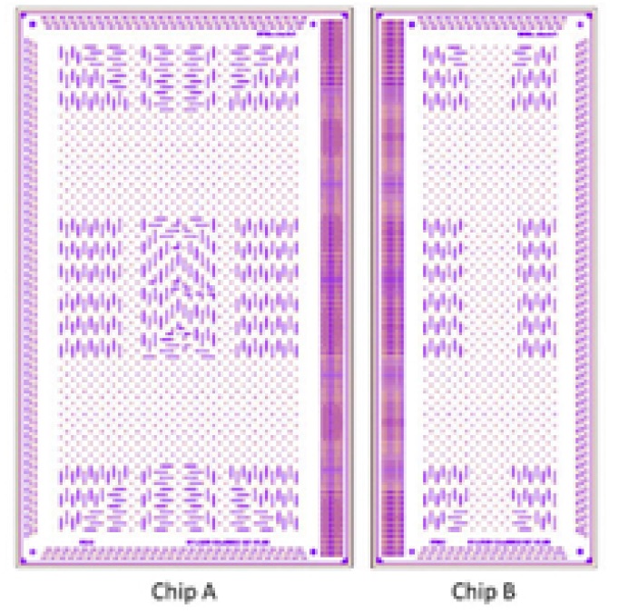
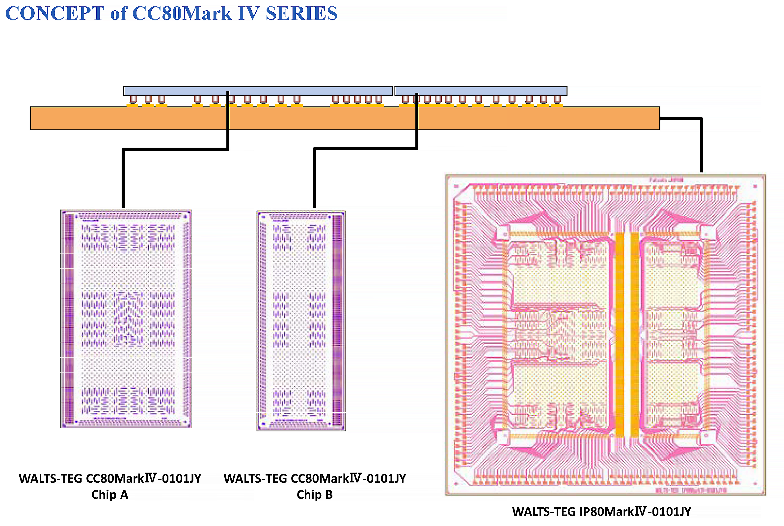
Practical Components CC80MarkIV-0101JY (A/B) advanced test wafer
Silicon Interposer for CC80MarkIV-101JY (A/B (IP80-0101JY)
Chip Structure
- Base Layer : P-TEOS
- Metal Layer : TiN / AI-0.5%Cu
- Passivation Layer : HDP / P-SiN
*TEOS : Tetraethoxysilane
*HDP : High Density Plasma
| Specifications | ||
| Wafer Size | 8 inch | |
| Wafer Thickness | 725±25μm | |
| Chip | A | B |
| Chip Size | 6.0mm x 10.0mm | 4.0mm x 10.0mm |
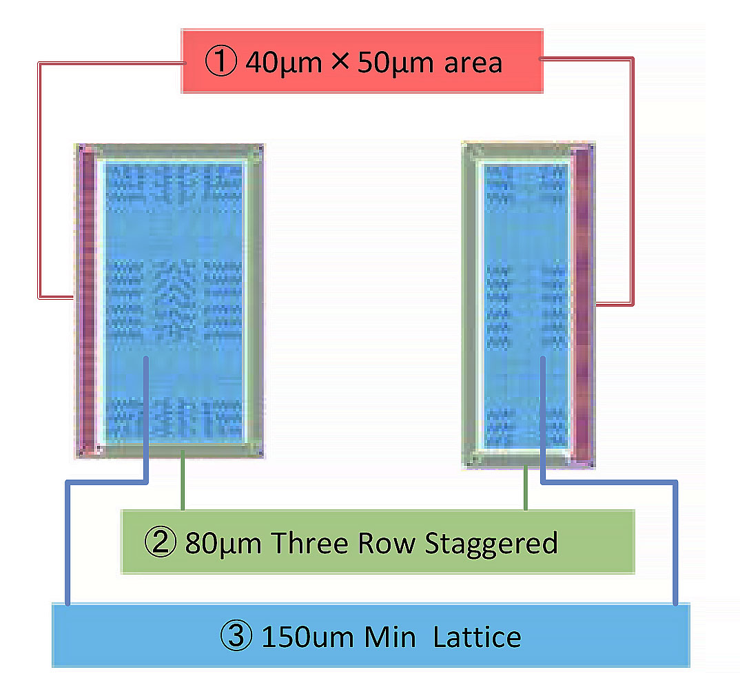
| Pad Pitch |
1. 40μm [10Row] x 50μm[192Row] (Peripheral) |
|
| Function | Daisy Chian | |
| Electrode/Height | Cu15um+SnAgum | |
| Pad Size | 1. 30μm 2. 30μm 3. 30μm |
|
| Passivation Opening |
12μm (Octagon) |
|
| Bump Size | φ25μm | |
| Number of Bump/Pad | 1. 1920 bumps / 1920 pads 2. 687 bumps / 687 pads 3. 1743 bumps / 1743 pads |
1. 1920 bumps / 1920 pads 2. 531 bumps / 531 pads 3. 978 bumps / 978 pads |
| Scribe Width | 120μm | |
| Number of Chip | Chip A: 228 chips/wafer | Chip B: 228 chips/wafer |